COURSE OUTCOMES:
Upon the successful completion of this course, the students will be able to,
CO1: Design and analyze the Printed Circuit Boards fabrication
CO2: Develop the Printed Circuit Boards and discuss the factors affecting PCB performance
COURSE CONTENT:
Introduction to PCB design - Basics of hardware and software - Types of PCB,
terminologies, PCB Layers - Different tools and software used for PCB designing -
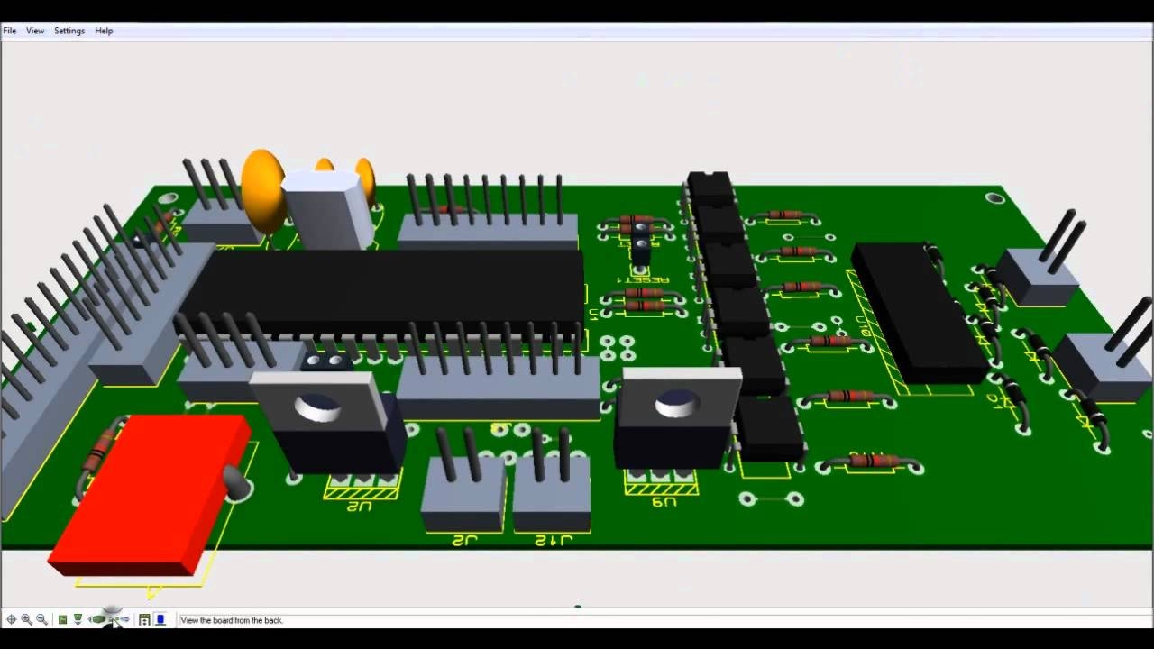
Different circuit on PCB design software - Creating a new project Building parts and symbols - Schematic of Different circuits - Creating multi-sheet flat designs - PCB layout
and 3D Imaging - Introduction to Proteus and OrCAD Capture - Placement of
components and Routing - Assigning reference designators - Design Rules checking -
Adding inter sheet signal references - PCB stackup preparation-Characteristics
impedance calculation-Signal Integrity analysis - Creating a Bill of Materials and Print
layout - Gerber generation - PCB fabrication methods - Soldering Methods.
L: 5 P: 20 TOTAL: 25 PERIODS
REFERENCES:
1. Charles Hamilton, “A Guide to Printed Circuit Board Design” Elsevier, 2013.
2. Kraig Mitzner, “Complete PCB Design Using OrCAD Capture and PCB Editor” Newnes Publications, 2009.
3. Christopher T. Robertson, “Printed Circuit Board Designer's Reference” Prentice Hall Professional, 2004.
4. Eric Bogatin, “Signal integrity analysis simplified”, Prentice Hall Modern Semiconductor Design Series, 2012.
5. http://www.ece.ucsb.edu/Faculty/Johnson/ECE189/Mentor2007/
- Teacher: ANTONY JEFFREY VAZ F